Application of Voltage Amplifiers in Guided Wave Propagation Experiments of PZT Transducers
Experiment Name: Guided Wave Propagation and Debonding/Delamination Validation Experiment Based on HSP Specimens and PZT Transducers
Research Direction: Investigate the correlation mechanism between high-frequency guided wave dispersion characteristics and debonding/delamination damage in honeycomb sandwich panels (HSP) and optimize monitoring methods. A periodic structural model is constructed using the equivalent conversion method, combined with simulations to quantify the influence of guided wavelength and honeycomb core scale on dispersion characteristics. Furthermore, the "debonding-induced shunting" propagation characteristics of high-frequency guided waves are validated through a solid finite element model and PZT sensing experiments, revealing the damage-sensitive mechanism where debonding/delamination leads to a significant increase in the amplitude of the A₀ mode. A method using the time-domain response of the high-frequency excited A₀ mode as a characteristic parameter is proposed to achieve precise identification of debonding/delamination, providing high-sensitivity, low false-alarm-rate engineering solutions for structural health monitoring of HSP in fields such as rail transportation and aerospace.
Experimental Objective: First, explore the influence of the ratio of guided wavelength to the side length of the honeycomb core unit cell on dispersion characteristics, guided wave mode propagation paths, and energy distribution in honeycomb sandwich panels through theoretical modeling and finite element simulations. Subsequently, based on a solid finite element model and PZT sensing experiments, design a validation scheme for the "shunting effect" of guided waves caused by debonding/delamination. Through comparative experiments on aluminum HSP specimens and prefabricated debonding areas, quantify the changes in the time-domain amplitude characteristics of the A₀ mode under debonding conditions and verify the sensitivity and reliability of high-frequency guided waves in identifying debonding damage.
Test Equipment: Signal generator, oscilloscope, ATA-2021B high-voltage amplifier, PZT transducers, HSP specimens, computer, etc.
Experimental Procedure: First, computer simulations were used to model the propagation of acoustic waves in honeycomb sandwich panels. It was found that when the acoustic wavelength is less than five times the size of the honeycomb cell, the acoustic waves concentrate on the surface of the material, and traditional theoretical models become invalid. Based on this finding, aluminum honeycomb panel specimens with prefabricated "debonding" damage were prepared, and an array of seven miniature sensors was arranged on the specimen surface. A 100 kHz detection acoustic wave generated by the signal generator was amplified to drive the sensors for wave emission and reception of the returned signals.

Figure 1: Physical Setup of the Experimental System

Figure 2: Block Diagram of the Experimental System
Experimental Results: When acoustic waves passed through the debonding area, the amplitude of a specific mode (A₀ mode) increased significantly by 48%, while the energy of other waveforms attenuated by 35%. This "amplitude increase" phenomenon was proportional to the size of the debonding area and served as a clear signal for identifying hidden damage. Through repeated tests, 100 kHz was determined to be the optimal detection frequency, with an A₀ mode amplitude increase of 30% set as the damage detection threshold.

Figure 3: Comparison of Time-Domain Signals Between Debonded and Healthy HSP

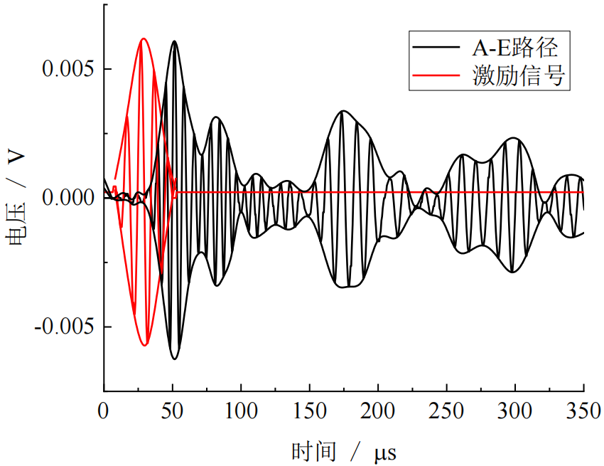
Figure 4: Comparison of Excitation and Sensing Signals

Figure 5: Dispersion Curves of HSP Structure
Role of the Amplifier in the Experiment: The signal amplifier employs a single-stage gain amplification mechanism to boost the milliwatt-level excitation signal from the signal generator to a volt-level driving voltage. This drives the PZT piezoelectric ceramic actuator to generate high-frequency guided waves, overcoming energy attenuation during guided wave propagation in the HSP structure and ensuring that the damage characteristics of debonding-induced shunting are accurately captured by the sensors.
Aigtek ATA-2021B High-Voltage Amplifier:

Figure: Specifications of the ATA-2021B High-Voltage Amplifier
The experimental materials in this article were compiled and published by Xi’an Aigtek Electronics. Xi’an Aigtek Electronics is a high-tech enterprise specializing in the research, development, production, and sales of electronic testing instruments, including power amplifiers, high-voltage amplifiers, power signal sources, preamplifiers for weak signals, high-precision voltage sources, and high-precision current sources. The company is committed to developing testing solutions for related industries centered on products such as power amplifiers, power signal sources, and metrology calibration sources, providing users with competitive testing solutions. Aigtek has become a large-scale instrument and equipment supplier in the industry with an extensive product line, and all demo units are available for free trial.
Hot News
-
Application of Voltage Amplifier in Stick-Slip Piezoelectric Actuator Experiments
-
Application of Voltage Amplifier in Research on Longitudinal Wave Sensors in Optical Fibers Based on Remote FBG
-
Application of ATA-1220E Broadband Power Amplifier in Research on Implantable Devices
-
Application of High-Voltage Power Amplifier in Performance Testing and Closed-Loop Experiments of Ultrasonic Motors
-
Application of Broadband Power Amplifier in Dynamic Characteristic Testing and Calibration Experiments of Heat Flux Sensors
-
Application of ATA-68020 Power Amplifier in Temperature Drift Compensation Experiment of Ultrasonic Motor


